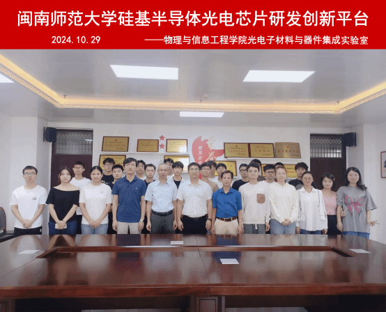
硅基半导体光电芯片研发创新团队
——光电子材料与器件集成实验室&微电子工艺实验室
光电子材料与器件集成实验室&微电子工艺实验室于2019年筹划建立。实验室聚焦于微电子与光电子专业相关的多个前沿方向,包括传统半导体薄膜材料、二维材料、纳米材料、红外光电探测器、红外激光器、集成电路及太阳能电池等。
截至目前,实验室已承担近20项科研项目,包括企业关键技术开发项目(500万元)、国家自然科学基金、省市级自然科学基金等,累计到账经费约400万元。已发表SCI、EI等高水平论文100余篇,授权专利15项。近五年来,指导学生在创新创业训练计划项目中获国家级立项2项、省级立项4项,并在各类专业竞赛中获得省级以上奖项20余项。
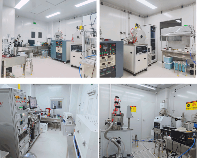
闽南师范大学近年来持续加大对光电子专业的支持力度,并逐步拓展至微电子领域。现已建成三个较为成熟的光电子与微电子实验室:“光电子材料与器件集成实验室”“微电子工艺实验室”和“硅基光电芯片研发实验室”。实验室均按微电子器件工艺的无尘化要求高标准设计和建设。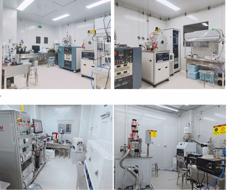
团队成员:
柯少颖(团队负责人):博士、教授、硕士生导师、院长助理;闽江学者青年学者、福建省C类人才、龙江计划拔尖人才、国家一流本科课程负责人、福建省一流本科课程负责人、微电子科学与工程专业负责人、物信学院教工第二支部书记;主持国家自然科学基金面上和青年项目各1项、闽江学者人才项目1项、福建省自然科学基金面上项目2项、漳州市自然科学基金1项、横向项目6项;研究方向:硅基光电子材料与红外探测器、雪崩光电探测器、半导体材料键合;以第一作者或通讯作者发表SCI论文60余篇,授权发明专利11项;近3年内指导本科生毕业论文8次被评为优秀毕业论文,指导本科生发表SCI论文5篇、EI论文10篇;获得第十四届福建省自然科学优秀学术论文三等奖、闽南师范大学优秀共产党员、闽南师范大学2020年度青年五四奖章。
周锦荣:副教授,硕士生导师,研究方向:光电半导体材料特性及其应用、光电控制与智能信息处理。主持福建省自然科学基金1项、福建省资助省属高校科研专项1项、福建省教育厅产学研合作项目1项、漳州市重大科技专项1项、教育部产学合作协同育人项目4项、横向项目4项等;目前已在国内外期刊发表论文30余篇,获得福建省自然科学优秀学术论文三等奖2项。指导学生获得国家级大学生创新创业训练计划项目3项、福建省大学生创新创业训练计划项目10项;指导学生参加各类专业竞赛获得国家一等奖3项、国家二等奖4项、国家三等奖2项,省级一等奖21项,省级二等奖21项等。荣获福建省优秀教师、漳州市优秀党务工作者、漳州市第六批优秀青年科技人才、闽南师范大学优秀共产党员等荣誉称号。
黄志伟:博士,副教授,研究方向:锗硅光电探测器研制、Si基二维材料与器件制备、近红外局域表面等离激元研究。近5年主持福建省自然科学基金1项、闽南师范大学科技项目2项。在硅基异质外延、近红外肖特基光电二极管、宽光谱红外探测器、表面等离子激元等方面已取得显著成果。目前已在国内外知名期刊(IEEE Journal of Lightwave Technology、IEEE Transactions on Electron Devices、Optics Express、Materials Science and Engineering B等)发表20余篇半导体材料及器件制备论文。
陈赐海:博士,教授,硕士生导师,电子系系主任,研究方向:光电信息材料与器件,印刷电子。研究对象:薄膜晶体管,存储器,智能传感电子,微能量收集与系统自供电等。主持福建省自然科学基金项目2项、省自然科学基金指导性项目1项、闽南师范大学科技项目2项,校企合作项目1项,参与国家863计划和国家重点研发计划课题项目,国家自然科学基金,省级科技创新重点项目等。已在国内外期刊(J. Mater. Chem. C、IEEE Trans. Electron Devices、Optics Lett.、ACS Appl. Mater. Interfaces等)发表论文20余篇,申报专利5项。
刘冠洲:博士,副教授,硕士生导师,曾任天津三安光电有限公司高级工程师,负责GaAs光伏芯片、硅基二极管、硅基三极管器件的研发与生产,参与GaAs基LED与LD芯片的研发,具有10年的半导体光电芯片行业从业经验。研究方向:二维材料与器件制备、GaAs基多结太阳能电池。主持福建省中青年重点项目1项,主持天津市科技支撑项目1项、天津市工业科技开发专项资金项目1项,授权发明专利10项。
团队成员主要科研项目
序号 | 项目名称 | 项目类别 | 项目经费(万元) | 研究起始时间 | 负责人 |
1 | Si基InP赝衬底匹配外延GeSn机理及GeSn中波红外线阵探测器研究 | 国家自然科学基金面上项目 | 54 | 2026.01-2029.12 | 柯少颖 |
2 | 全键合长波长InGaAs/Si单光子雪崩探测器基础研究 | 国家自然科学基金青年项目 | 24 | 2021.01-2023.12 | 柯少颖 |
3 | 硅基半导体异质结构光电探测器研究 | “闽江教育领军人才”闽江学者青年学者 | 100 | 2025.02-2028.02 | 柯少颖 |
4 | InP-O-I基高Sn组分GeSn薄膜外延生长及其中红外探测性能研究 | 福建省自然科学基金面上项目 | 10 | 2024.11-2027.11 | 柯少颖 |
5 | Si基GeSn短波红外全光谱PIN光电探测器基础研究 | 福建省自然科学基金面上项目 | 7 | 2021.01-2023.12 | 柯少颖 |
6 | InGaAs/Si异族键合基础研究 | 漳州市自然科学基金 | 2 | 2020.01-2022.12 | 柯少颖 |
7 | 锗硅微光CMOS图像传感显示模块雏形研发 | 横向项目 | 100 | 2022.01-2023.7 | 柯少颖 |
8 | 单晶XXX化合物制备及其光电器件开发 | 横向项目 | 20 | 2024.07-2027.07 | 柯少颖 |
9 | 硅基分子束外延XXX工艺技术开发 | 横向项目 | 20 | 2024.04-2025.04 | 柯少颖 |
10 | 半导体XXX芯片工艺开发与芯片加工 | 横向项目 | 20 | 2023.10-2025.10 | 柯少颖 |
11 | 原子层沉积工艺技术开发 | 横向项目 | 3.7 | 2023.07-2023.12 | 柯少颖 |
12 | 单晶二维材料制备与转移技术开发 | 横向项目 | 4.7 | 2022.11-2023.12 | 柯少颖 |
13 | 基于键合材料高性能ITO/Si基n-Ge肖特基光电探测器的研制 | 福建省自然科学基金项目 | 8 | 2023.01-2025.01 | 黄志伟 |
14 | 近红外局域表面等离激元共振增强Ge肖特基光电探测器基础研究 | 闽南师范大学高级别培育项目 | 2 | 2022 | 黄志伟 |
15 | ITO/Ge、ITO/Si肖特基光电二极管的研制 | 闽南师范大学校长基金 | 10 | 2020 | 黄志伟 |
16 | 新工科背景下信息类在线实践教学应用研究 | 教育部产学合作协同育人项目 | 5 | 2021.04-2022.12 | 周锦荣 |
17 | 智慧路灯NB-IOT智能控制系统 | 校企合作项目 | 15 | 2020.01-2022.03 | 周锦荣 |
18 | 虚实结合的通信原理实验教学设计研究 | 教育部产学合作协同育人项目 | 3 | 2019.10-2020.11 | 周锦荣 |
19 | 光电信息专业实践教学改革探索与实践 | 教育部产学合作协同育人项目 | 3 | 2019.10-2021.03 | 周锦荣 |
20 | DSP教学应用研究与实践 | 教育部产学合作协同育人项目 | 2 | 2019.01-2020.04 | 周锦荣 |
21 | 物联网智能云实验室建设 | 漳州市科技重大专项 | 40 | 2017.12-2020.09 | 周锦荣 |
22 | 功率型白光LED自动反馈补偿智能调光系统模型研究 | 福建省自然科学基金面上项目 | 4 | 2016.04-2019.01 | 周锦荣 |
23 | 功率型LED非线性调光系统应用研究 | 资助省属高校科研专项 /福建省教育厅产学研科技项目 | 4 | 2016.06-2018.02 | 周锦荣 |
24 | 光电探测成像智能调控系统研制 | 横向项目 | 15 | 2025.05-2026.12 | 周锦荣 |
25 | 基于二维材料的光电探测器研制 | 横向项目 | 3 | 2025.05-2026.06 | 周锦荣 |
26 | 智慧路灯NB-IOT智能控制系统 | 横向项目 | 15 | 2020.01-2022.03 | 周锦荣 |
27 | 便携式摄影专业监视器开发 | 横向项目 | 0.9 | 2014.04-2015.04 | 周锦荣 |
28 | 硅基InGaAs红外光电探测器基础研究 | 福建省中青年重点项目 | 10 | 2024 | 刘冠洲 |
29 | 高效化合物多结太阳能电池 | 闽南师范大学校长基金 | 10 | 2021 | 刘冠洲 |
30 | 倒装多结太阳电池芯片工艺开发 | 天津市科技支撑项目 | 30 | 2016 | 刘冠洲 |
31 | 空间用UMM结构三结太阳能电池外延及芯片工艺 | 天津市工业科技开发专项资金项目 | 65 | 2016 | 刘冠洲 |
32 | 印刷突触晶体管光电调控感知机制及逻辑行为研究 | 福建省自然科学基金面上项目 | 7 | 2021.11-2024.11 | 陈赐海 |
33 | 基于喷墨打印技术的薄膜晶体管制备及其应用研究 | 福建省自然科学基金面上项目 | 6.5 | 2017.04-2020.04 | 陈赐海 |
34 | 谐振腔电磁计算方法及其在材料检测中应用 | 福建省自然科学基金指导性项目 | 3 | 2012.12-2015.12 | 陈赐海 |
35 | OLED显示驱动单元的微型化与柔性化 | 横向项目 | 4.8 | 2020.1-2023.1 | 陈赐海 |
36 | 溶液法制备半导体阵列及其器件研究 | 校长基金 | 5 | 2020.12-2024.12 | 陈赐海 |
37 | 无源驱动白光LED照明系统的动态能量传递机理及瞬态混合光调制特性 | 国家自然科学基金面上(参与) | 59 | 2020.1-2023.12 | 陈赐海 |
38 | 低能耗小间距全彩LED显示模组关键技术及产业化 | 省科技创新重点项目(参与) | 100 | 2022.07-2025.07 | 陈赐海 |
团队成员发表的主要论文
柯少颖论文
[1] SHI, Z. W., et al. InGaAs/Si Avalanche Photodiode With High Gain and Low Dark Current Achieved by Two-Step Wafer Bonding. *IEEE Transactions on Electron Devices*, 2025.
[2] DIAO, Y. L., et al. Magnetron sputtering growth and growth mechanism of GeSn films with Sn content exceeding 25% on InP substrates. *Applied Surface Science*, 2025, 699: 163122.
[3] WANG, Z. R., et al. High-Gain Ge/Si Avalanche Photodetector With Stable Operation Temperature Up to 500 K. *IEEE Electron Device Letters*, 2025.
[4] MENG, W. H., et al. High-speed low-noise InGaAs/InP PIN photodetectors on a Si platform achieved by oxygen plasma activation bonding. *Optics Letters*, 2025, 50(11): 3549–3552.
[5] XU, X. J., et al. Selenization Mechanism of Nearly 4 in. Single-Oriented PtSe₂ and PtSe₂/n–-Si/n⁺-Si 2D–3D PIN Wide-Spectrum Polarization Detectors. *ACS Applied Materials & Interfaces*, 2025, 17(20): 29910–29922.
[6] XU, X. J., et al. Stable Self-Powered Broadband PtSe₂/Si Pin Infrared Photodetector Based on a High-Quality Ultrapure Intrinsic Si Film Exfoliated by Si/SOI Wafer Bonding. *ACS Applied Materials & Interfaces*, 2025, 17(10): 15579–15592.
[7] LIU, B., et al. Quantum-Confined 0D/2D/3D Heterostructure Photodetectors with an Ultrafast Self-Powered Broadband Response for Short-Wave Infrared Imaging. *ACS Applied Materials & Interfaces*, 2025.
[8] KE, S. Q., et al. In Situ Selenization Engineered Dual Schottky Heterojunctions: A Novel Architecture for High‐Speed Broadband Photonic Communication Detector Arrays. *Small*, 2025: e07077.
[9] LI, J. H., et al. Fabrication of a high-performance Ge/Si PIN photodetector utilizing Ge/Si hetero-bonding with a microcrystalline Ge interlayer. *Optics Express*, 2024, 32(27): 48858–48874.
[10] SHI, Z. W., et al. Double modulation of the electric field in InGaAs/Si APD by groove rings for the achievement of THz gain-bandwidth product. *Physica Scripta*, 2024, 99(11): 115501.
[11] CHEN, S. P., et al. High-Speed Self-Powered PdSe₂/Si 2D-3D PIN-like Photodetector with Broadband Response Based on PdSe₂ Quantum Island Structure. *ACS Applied Materials & Interfaces*, 2024, 16(32): 42577–42587.
[12] YE, S. M., et al. Microstructure and ferromagnetism of Mn₀.₀₅Ge₀.₉₅ quantum dots/graphene heterostructures for spintronic devices. *ACS Applied Nano Materials*, 2024, 7(14): 16542–16552.
[13] JI, T., et al. High-speed broadband PtSe₂/Si 2D-3D pin photodetector with a lightly n-doped Si interlayer based on single-oriented PtSe₂. *ACS Photonics*, 2024, 11(8): 3150–3159.
[14] SUN, Z. W., et al. Nanometer-thick CsPbBr₃ films with embedded CsPb₂Br₅ nanowires for photodetector applications. *ACS Applied Nano Materials*, 2024, 7(10): 11785–11793.
[15] KE, S. Y., et al. Achievement of non-charge layer InGaAs/Si avalanche photodiodes by introducing a groove ring at the bonding interface. *Physica Scripta*, 2024, 99(5): 055006.
[16] WU, D. Z., et al. Microstructure and room temperature ferromagnetism of double-layered MnₓGe₁−ₓTe polycrystalline modified by the space-layer thickness. *Applied Surface Science*, 2024, 657: 159837.
[17] WANG, J., et al. Interface characteristics of InP/Si heterojunction fabricated by low-temperature wafer bonding based on microcrystalline Ge interlayer. *Vacuum*, 2024, 223: 113103.
[18] TAN, C. H., et al. Growth of single-crystalline GeSn films with high-Sn content on InP substrates by sputtering and rapid thermal annealing. *Applied Surface Science*, 2024, 657: 159707.
[19] YAO, L. Q., et al. Low dark current lateral Ge PIN photodetector array with resonant cavity effect for short wave infrared imaging. *Journal of Physics D: Applied Physics*, 2024, 57(16): 165103.
[20] CHEN, X. P., et al. Low voltage-driven, high-performance TiO₂ thin film transistors with MHz switching speed. *RSC Advances*, 2024, 14(9): 6058–6063.
[21] BAO, S. Y., et al. High-gain bandwidth product of wafer-bonded near-infrared III-V/silicon APD using polycrystalline silicon bonding layer. *Physica Scripta*, 2023, 98(12): 125527.
[22] HUANG, Y., et al. Bonding mechanisms and electrical properties of Ge/Si and Si/Si bonded wafers achieved by thin microcrystalline Ge interlayer. *Journal of Alloys and Compounds*, 2023, 965: 171485.
[23] LI, J., KE, S., WANG, J., et al. High-quality Ge/Si hetero-bonding by sputtered microcrystalline Ge interlayer. *Vacuum*, 2023: 112203.
[24] LIN, G., QIAN, K., DING, H., …, KE, S., et al. Effective strain relaxation of GeSn single crystal with Sn content of 16.5% on Ge grown by high-temperature sputtering. *Applied Surface Science*, 2023, 623: 157086.
[25] JIAO, J., CHEN, X., RAO, Y., …, KE, S., et al. High-quality InGaAs films bonded on Si substrate with a thin polycrystalline Si intermediate layer. *Applied Surface Science*, 2023, 628: 157296.
[26] CHAI, J., KE, S., HUANG, Y., et al. Effect of bubbles at the bonded interface on the performance of GeSn/Si PIN photodetector. *Physica Scripta*, 2023, 98(6): 065517.
[27] CHEN, X., JIAO, J., YAO, L., …, KE, S., et al. Effect of the bonding layer and multigrading layers on the performance of a wafer-bonded InGaAs/Si single-photon detector. *Applied Optics*, 2023, 62(12): 3125–3131.
[28] KE, S., XIAO, X., JIAO, J., et al. Theoretical achievement of THz gain-bandwidth product of wafer-bonded InGaAs/Si avalanche photodiodes with poly-Si bonding layer. *IEEE Transactions on Electron Devices*, 2022, 69(3): 1123–1128.
[29] KE, S., LI, J., WANG, J., et al. Blocking of Ge/Si lattice mismatch and fabrication of high-quality SOI-based Ge film by interlayer wafer bonding with polycrystalline Ge bonding layer. *Vacuum*, 2022, 203: 111269.
[30] LI, X., WANG, Y., CHEN, T., et al. Unencapsulated CsPbClBr₂ Film Photodetectors Grown by Thermal Vacuum Deposition Exhibit Exceptional Environmental Stability in High-Humidity Air. *ACS Applied Energy Materials*, 2022, 5(7): 8709–8716.
[31] HUANG, D., JI, R., YAO, L., …, KE, S., et al. Strain-induced abnormal Ge/Si inter-diffusion during hetero-epitaxy process. *Vacuum*, 2022, 196: 110735.
[32] HUANG, D., JI, R., YAO, L., …, KE, S., et al. Dislocation nucleation triggered by thermal stress during Ge/Si wafer bonding process at low annealing temperature. *Applied Surface Science*, 2021, 568: 150979.
[33] LI, Z., HUANG, D., JIAO, J., …, KE, S., et al. Effect of the thermal stress on the defect evolution at GaAs/Si wafer bonding with a-Ge intermediate layer. *Semiconductor Science and Technology*, 2021, 36(9): 095005.
[34] KE, S., CHEN, Z., ZHOU, J., et al. Theoretical prediction of high-performance room-temperature InGaAs/Si single-photon avalanche diode fabricated by semiconductor interlayer bonding. *IEEE Transactions on Electron Devices*, 2021, 68(4): 1694–1701.
[35] KE, S., LI, D., CHEN, S. A review: wafer bonding of Si-based semiconductors. *Journal of Physics D: Applied Physics*, 2020, 53(32): 323001.
[36] KE, S., ZHOU, J., WANG, Z., et al. Double intermediate bonding layers for the fabrication of high-quality silicon-on-insulator-based exfoliated Ge film with excellent high-temperature characteristics. *Journal of Physics D: Applied Physics*, 2020, 53(16): 165109.
[37] KE, S., ZHOU, J., HE, S., et al. Bubble evolution mechanism and defect repair during the fabrication of high-quality germanium on insulator substrate. *Semiconductor Science and Technology*, 2020, 35(3): 035012.
[38] KE, S., ZHOU, J., HUANG, D., et al. Polycrystalline Ge intermediate layer for Ge/Si wafer bonding and defect elimination in Si (SOI)-based exfoliated Ge film. *Vacuum*, 2020, 172: 109047.
[49] KE, S., YE, Y., WU, J., et al. Low-temperature fabrication of wafer-bonded Ge/Si pin photodiodes by layer exfoliation and nanosecond-pulse laser annealing. *IEEE Transactions on Electron Devices*, 2019, 66(3): 1353–1360.
[40] KE, S., YE, Y., WU, J., et al. Interface characteristics of different bonded structures fabricated by low-temperature a-Ge wafer bonding and the application of wafer-bonded Ge/Si photoelectric device. *Journal of Materials Science*, 2019, 54(3): 2406–2416.
[41] KE, S., YE, Y., LIN, S., et al. Low-temperature oxide-free silicon and germanium wafer bonding based on a sputtered amorphous Ge. *Applied Physics Letters*, 2018, 112(4): 041601.
[42] KE, S., YE, Y., WU, J., et al. Interface characteristics and electrical transport of Ge/Si heterojunction fabricated by low-temperature wafer bonding. *Journal of Physics D: Applied Physics*, 2018, 51(26): 265306.
[43] KE, S., LIN, S., YE, Y., et al. Temperature-dependent interface characteristic of silicon wafer bonding based on an amorphous germanium layer deposited by DC-magnetron sputtering. *Applied Surface Science*, 2018, 434: 433–439.
[44] KE, S., LIN, S., HUANG, W., et al. Geiger mode theoretical study of a wafer-bonded Ge on Si single-photon avalanche photodiode. *Journal of Physics D: Applied Physics*, 2017, 50(5): 055106.
[45] KE, S., LIN, S., YE, Y., et al. Bubble evolution mechanism and stress-induced crystallization in low-temperature silicon wafer bonding based on a thin intermediate amorphous Ge layer. *Journal of Physics D: Applied Physics*, 2017, 50(40): 405305.
[46] KE, S., LIN, S., MAO, D., et al. Interface state calculation of the wafer-bonded Ge/Si single-photon avalanche photodiode in Geiger mode. *IEEE Transactions on Electron Devices*, 2017, 64(6): 2556–2563.
[47] KE, S., LIN, S., LI, X., et al. Voltage sharing effect and interface state calculation of a wafer-bonding Ge/Si avalanche photodiode with an interfacial GeO₂ insulator layer. *Optics Express*, 2016, 24(3): 1943–1952.
[48] KE, S., YE, S., YANG, J., et al. Morphological evolution of self-assembled SiGe islands based on a mixed-phase pre-SiGe island layer grown by ion beam sputtering deposition. *Applied Surface Science*, 2015, 328: 387–394.
黄志伟论文
[1] Ge Y, Huang Z*, et al. 300–2200 nm broadband Si Schottky photodetectors with ultra-low dark current (<10 nA/cm²) via Al₂O₃/SiOₓ interface engineering[J]. IEEE Journal of Lightwave Technology, 2025, 43: 8832.
[2] Ge Y, Huang Z*, Yang M, et al. 532–2200 nm Si Schottky photodetectors featuring nonuniform barrier layers[J]. IEEE Transactions on Electron Devices, 2025, 72: 3667.
[3] Ke S, Wang J, Huang Z*, et al. Achievement of non-charge layer InGaAs/Si avalanche photodiodes by introducing a groove ring at the bonding interface[J]. Physica Scripta, 2024, 99(5): 055006.
[4] Jiang R, Chen F, Zheng Z, Ke S, Zhou J, Liu G, Huang Z*. Simulation and analysis of extinction properties of Rh nanostructures[J]. Laser & Optoelectronics Progress, 2023, 60(19): 1925001.
[5] Chen F, Jiang R, Zheng Z, Ke S, Zhou J, Liu G, Huang Z*. Simulation and analysis of infrared extinction characteristics of ITO nanorod structures[J]. Acta Optica Sinica, 2023, 43(9): 0916002.
[6] Huang Z, et al. High-performing silicon-based germanium Schottky photodetector with ITO transparent electrode[J]. Chinese Physics B, 2021, 30(3): 037303.
[7] Huang Z, Wang J, Huang W, et al. Research progress of technologies for germanium near-infrared photodetectors[J]. Infrared and Laser Engineering, 2020, 49(1): 0103004.
[8] Huang Z, Yu C, Chang A, et al. High-k dielectric interlayered ITO/germanium Schottky photodiodes with low dark current and high photoconductive gain[J]. Journal of Materials Science, 2020, 55(20): 8630-8641.
[9] Yu C, Huang Z, et al. High-specific-detectivity, low-dark-current Ge nanowire metal–semiconductor–metal photodetectors fabricated by Ge condensation method[J]. Journal of Physics D: Applied Physics, 2020, 53(12): 125103.
[10] Huang Z, Mao Y, Lin G, et al. Impacts of ITO interlayer thickness on metal/n-Ge contacts[J]. Materials Science and Engineering: B, 2017, 224: 103-109.
[11] Huang Z, Mao Y, Lin G, et al. Low dark current broadband 360-1650 nm ITO/Ag/n-Si Schottky photodetectors[J]. Optics Express, 2018, 26(5): 5827-5834.
[12] Huang Z, Mao Y, Chang A, et al. Low-dark-current, high-responsivity indium-doped tin oxide/Au/n-Ge Schottky photodetectors for broadband 800-1650 nm detection[J]. Applied Physics Express, 2018, 11(10): 102203.
[13] Huang Z, et al. Impacts of excimer laser annealing on Ge epilayer on Si[J]. Applied Physics A, 2017, 123(2): 148.
[14] Huang Z, et al. Suppressing the formation of GeOₓ by doping Sn into Ge to modulate the Schottky barrier height of metal/n-Ge contact[J]. Applied Physics Express, 2016, 9(2): 021301.
周锦荣论文
[1] [1]Chen S, Ke S,…Zhou J*, et al. High-Speed Self-Powered PdSe2/Si 2D-3D PIN-like Photodetector with Broadband Response Based on PdSe2 Quantum Island Structure.ACS applied materials & interfaces,2024,Vol.16(32): 42577-42587.
[2] Zhou J, Bao S, …Ke S, et al. Effect of a-Si1-xGex Bonding Layer with Different Ge Compositions on the Performance of InGaAs/Si Avalanche Photodiode. Acta Photonica Sinica,2022,51(09):126-135.
[3] 彭强, 柯海鹏, …周锦荣*等. Ge/Si异质键合界面纳米级氧化层对Ge/Si异质结光电特性调控机制, 硅酸盐学报, 2021, 49(01):180-188.
[4] 周锦荣.功率型白光LED的非线性混合调光方法研究等, 发光学报, 2017, 38(9): 1249-1255.
[5] 周锦荣,陈焕庭,周小方. 白光LED色温的非线性动态预测模型, 发光学报, 2016, 37(1): 106-111.
[6] 周锦荣.白光LED智能调光数学模型, 发光学报 2015, 36(8): 953-956.
刘冠洲论文
[1] Liu G Z, Li C, Lu C B, ...,Ke S, et al. Wet thermal annealing effect on TaN/HfO2/Ge metal-oxide-semiconductor capacitors with and without a GeO2 passivation layer. Chinese Physics B, 2012, 21(11): 117701.
[2] Liu G, Li C, Lai H, ...,Ke S, et al. Ge incorporation in HfO2 dielectric deposited on Ge substrate during dry/wet thermal annealing. Journal of the Electrochemical Society, 2010, 157(6): H603.
陈赐海论文
[1] [1] LV, Q.; et al. A Bioinspired Low-Power Optoelectronic Synaptic Transistor for Artificial Visual Recognition and Multilevel Optical Storage. ACS Appl. Mater. Interfaces 2025.
[2] LIU, G.; et al. Determining 2-D Optical Characteristics-Dependent Surface Temperature of Organic Light-Emitting Diode. IEEE Trans. Electron Devices 2023, *70*(12), 6427–6434.
[3] SHI, J.; et al. Optoelectronic Synaptic Transistors via Adding Insulator into Semiconductor for Brain-Inspired Computing. IEEE Trans. Electron Devices 2024.
[4] CHEN, C.; et al. Low-Temperature Solution-Processed Nanoparticle-Doped Nickel Oxide Thin-Film Transistor. J. Appl. Phys. 2023, *133*(5).
[5] LI, X.; et al. Effect of the Methane Flow Ratio on the Structural and Mechanical Properties of High-Entropy Alloy Co-Doped DLC Films. Diam. Relat. Mater. 2021, *117*, 108486.
[6] CHEN, C.; et al. Structure and Cutting Performance of Ti-DLC Films Prepared by Reactive Magnetron Sputtering. Diam. Relat. Mater. 2020, *104*, 107735.
[7] LI, X.; TANG, W.; CHEN, C.; et al. Effects of Sputtering Time on Structure and Mechanical Properties of (AlCrNb)N Coatings Deposited by High-Power Impulse Magnetron Cosputtering. JOM 2020, *72*(6), 2164–2173.
[8] CHEN, C.; YANG, Q.; CHEN, G.; et al. Solution-Processed Oxide Complementary Inverter via Laser Annealing and Inkjet Printing. IEEE Trans. Electron Devices 2019, *66*(11), 4888–4893.
[9] CHEN, C.; YANG, H.; YANG, Q.; et al. Low-Temperature Solution-Processed Flexible Metal Oxide Thin-Film Transistors via Laser Annealing. J. Phys. D: Appl. Phys. 2019, *52*(38), 385105.
[10] LI, X.; CHEN, C.; XU, C. Optimization of Interlayer/CrWN Bilayer Films Fabricated and Monitored under Shewhart Control. J. Mater. Eng. Perform. 2019, *28*(11), 6993–7005.
[11] LI, X.; et al. Effect of Annealing Treatment on the Structure and Performance of Transparent Conductive AZO/Al2O3 Bi-Layer Films. Mater. Res. Express 2019, *6*(9), 096414.
[12] SUN, D.; CHEN, C.; ZHANG, J.; et al. High Performance Inkjet-Printed Metal Oxide Thin Film Transistors via Addition of Insulating Polymer with Proper Molecular Weight. Appl. Phys. Lett. 2018, *112*(1), 012102.
[13] CHEN, C.; CHEN, G.; YANG, H.; et al. Solution-Processed Metal Oxide Arrays Using Femtosecond Laser Ablation and Annealing for Thin-Film Transistors. J. Mater. Chem. C 2017, *5*(36), 9273–9280.
[14] YANG, H.; CHEN, C.; et al. Solution Processed Organic Thin Film Transistor Arrays with Assistance of Laser Ablation. ACS Appl. Mater. Interfaces 2017, *9*(4), 3849–3856.
实验室团队成员获得授权发明专利:
(1) 一种利用微晶锗薄膜实现低温Si-Ge和Si-InP键合的方法,专利号202211165174.4
(2) 一种实现晶格阻断的零气泡Ge/Si异质混合集成方法,专利号201910940185.7
(3) 一种耐高温高质量SOI基剥离Ge薄膜的制备方法,专利号201910938320.4
(4) 一种提高剥离Si基和SOI基Ge薄膜质量的方法,专利号201910939228.X
(5) 一种无气泡坑超高质量SOI基Ge薄膜异质键合方法,专利号201910942951.3
(6) 一种无气泡无穿透位错 Ge/Si 异质混合集成方法,专利号201910944976.7
(7) 一种超高质量 SOI 基键合 Ge 薄膜的制备方法,专利号201910941003.8
(8) 集成旁路二极管的太阳电池及其制备方法. 专利号201310399140.6
(9) 一种多结太阳能电池的集成旁路二极管的制备方法. 专利号201510894699.5
(10) 一种多结太阳电池芯片的检测装置及检测方法. 专利号201610598963.5
(11) 一种外延缺陷处理设备. 专利号2018206425333
(12) 一种太阳能电池. 国际专利 S1038PCT/CN2018/087368
(13) 一种高压发光二极管及其制备方法. 专利号201811361047.5
(14) 一种多结太阳能电池. 专利号201910223921.7
(15) 一种砷化镓多结太阳能电池芯片及其制备方法. 专利号202011506396.9
(16) 一种太阳能电池芯片及其制作方法. 专利号202011586812.0
(17) 一种柔性太阳能电池组件及其制作方法. 专利号202011511065.4
(18) 一种通过双交联反应对有机薄膜晶体管绝缘层优化的方法.专利号201610768689.1
(19) 弱键合强度脆性键合样品截面透射电子显微镜制备方法,专利号201810347004.5
(20) 一种无界面气泡绝缘层上锗键合方法,专利号201810347003.0
(21) 利用非晶锗薄膜实现低温Si-Si键合的方法,专利号201710118093.1
(22) 集成旁路二极管的太阳电池及其制备方法. 专利号201310399140.6